
Maskless Laser Lithography
CAD-based prototyping
Contacts: Mr. Mark Oksman, mark.oksman@biu.ac.il
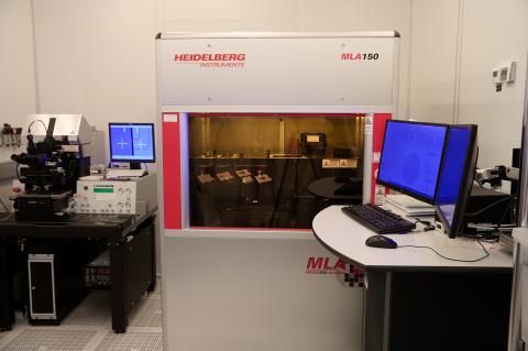
Model: MLA 150
Manufacture: Hiedelberg Instruments
Description:
The Maskless Aligner MLA 150 is a cutting-edge maskless lithography tool designed for rapid prototyping, R&D, and small-scale production. It is the fastest maskless lithography system available, offering unparalleled flexibility for applications such as quantum device fabrication (2D materials, semiconductors, nanowires, etc.), MEMS, micro-optics, sensors, actuators, MOEMS, and other material and life sciences technologies.
The MLA 150 enables high-resolution, high-aspect-ratio patterning and can even create grayscale structures depending on the application. It integrates two laser wavelengths (405 nm and 375 nm), allowing exposure of a wide range of photoresists.
Unlike traditional mask aligners, the MLA 150 eliminates the need for photomasks, significantly reducing turnaround times. Design modifications can be implemented immediately by simply updating the CAD layout and exposing the pattern directly.
Specifications:
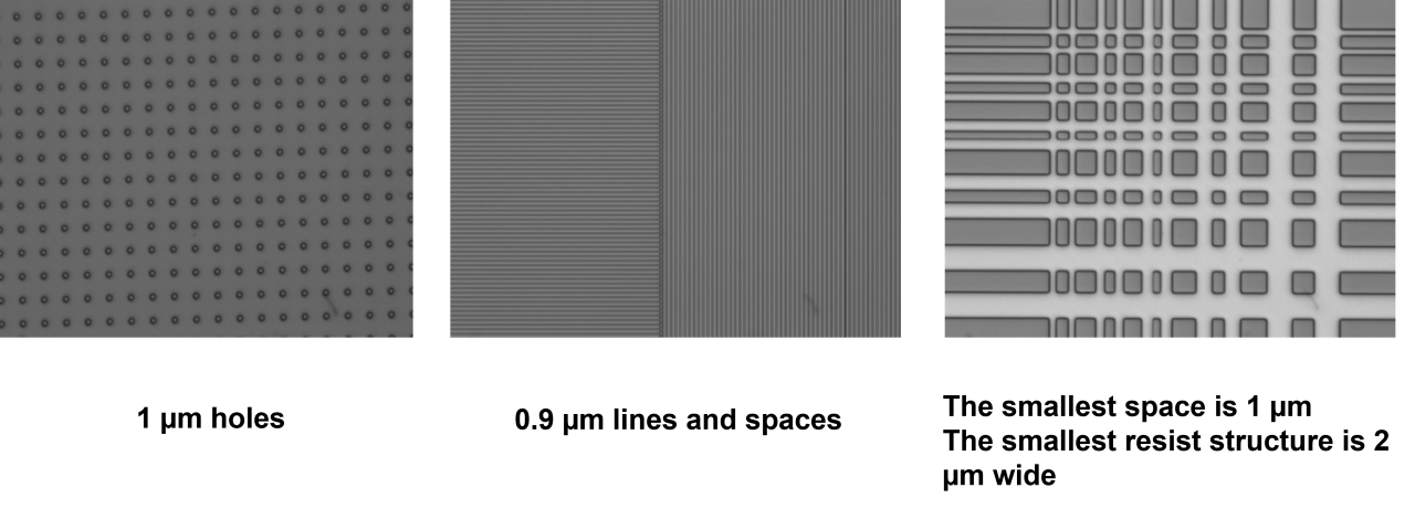
- Minimum structure size 1μm
- Linewidth variation [3σ] 120 nm
- Global 2nd layer alignment [3σ] 500 nm
- Local 2nd layer alignment [3σ] 250 nm
- Light source: Diode lasers 405 nm and 375 nm
- Exposure time 405 nm laser for 4“ wafer 9 min
- Exposure time 375 nm laser for 4“ wafer 20 min
- Max. write speed 375 nm laser 500 mm2 /min
- Max. write speed 405 nm laser 1100 mm2 /min
- Interferometric 200 mm x-y-Stage System with position resolution of 20 nm
- Min. Substrate Size 5 x 5 mm²
- Max. Substrate Size 200 x 200 mm²
- Substrate Thickness 0 to 12 mm
- Temperature controlled flow box Temperature stability ±0.1°
Last Updated Date : 25/06/2025