

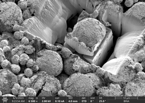
FIB (Helios600)
Nano-imaging, elemental composition analysis & high presicion milling, deposition at the nano and micro-scales
Dual-beam system combining SEM and FIB for high-resolution imaging, cross-sectioning, material analysis, and 3D reconstruction. Ideal for TEM sample prep, device modification, failure analysis, and tomography. Includes EDX and cryo-stage.
BINA's Characterization Unit welcomes both industry professionals and researchers – providing state-of-the-art equipment, expert support, and customized solutions. We’re here for you!
Contacts: Dr. Sasha Domantovsky, alexander.domantovsky@biu.ac.il
Model: Helios 5UC DualBeam
Manufacture: Thermo Fisher Scientific, USA
Resolution:
Electron beam: 0.6 nm at 15 kV; 1.2 nm at 1 kV
Ion beam at coincident point: 4.0 nm at 30 kV
Specifications:
- Electron beam current range: 1.6 pA to 100 nA
- Accelerating voltage range:350 V – 30 kV
- Ion beam current range: 1 pA – 100 nA
- Accelerating voltage range: 500 V – 30 kV
Analytical and imaging detectors:
- Secondary electrons detectors
- Secondary ions detector
- Backscattered electrons detectors
- Electron detector for STEM
- X-ray detector for energy-dispersive X-ray spectroscopy
Last Updated Date : 16/11/2025