Electromagnetism & Spintronics
The BINA Electromagnetism researchers study novel magnetic phenomena and develop advanced spintronic devices using magnetic nanoparticles, magnetic thin films, and heterostructures. They study the interplay of magnetism and superconductivity and explore the emergence of magnetic phenomena in strongly correlated materials and at various interfaces. The researchers use nanofabrication facilities to develop novel magnetic sensors and memory devices with immense potential impact on vital technologies. A significant effort of the researchers is related to medicine, where attempts are made to develop devices and procedures that harness magnetism for diagnosis and treatment.
- Magnetism and superconductivity
- Electronic systems
- Granular & thin films
- Magnetic nanomaterials
- Manganites
- Single-molecule and single-photon spectroscopy
- Meso- and nano-systems
- Spintronics
Researchers
-

Nano-scale crystallization phenomena
Our group is developing approaches that utilize nano-scale systems for studies of crystallization phenomena and mechanisms that determine the morphologies of crystals. Insight from this research can lead to very useful technological applications, as understanding crystal growth mechanisms will allow us to better control crystalline products of chemical synthesis. This view is inspired by treating nano-crystals as “embryonic” stages of crystal growth. In a sense, every crystal begins its evolution as a nano-crystal. The huge advantage in studies that follow this perspective is in our ability to utilize extremely powerful electron microscopy methods, including a novel technique that allows us to perform high resolution electron microscopy directly in liquid solutions. In this way we can retrieve details of the crystal structure and overall shape at remarkable resolution, during the crystal’s initial formation. These details are often hidden in bulk crystals, unidentifiable by X-ray crystallography, yet critical for understanding of the mechanisms by which crystals grow.
-

Prof. Aviad Frydman
972-3-531-8102
Electronic properties of low dimensional systems

• Thin film growth: Thermal evaporation, e-beam evaporation UHV techniques and quench- condensation methods.
• Advanced Lithography: Electron beam nano-lithography and Photo-lithography, ion milling, reactive ion milling, chemical etching and other processing techniques applicable to sub-micron electronics.
• Microscopy: Scanning and transmission electron microscopy, scanning tunneling microscopy (STM) and atomic force microscopy (AFM).
• Low Temperature: Cryogenic measurement techniques, low noise measurements, dc and ac (lock-in) techniques, high field magneto-transport measurements. -

Prof. Beena Kalisky
972-3-738-4339
Sensitive magnetic imaging
• Superconductivity
• Nano-magnetism
• Bio-magnetism
• Scanning SQUID microscopy
• Complex oxid interfaces
• Nano-electronics -

Prof. Lior Klein
972-3-531-7861
Multi-level magnetic memory

• Magneto-transport in thin magnetic films (particularly ruthenates and manganites)
• Anisotropic magnetoresistance and giant planar Hall effect
• Current induced manipulation of domain walls
• Macroscopic quantum tunneling
• Transport properties of LAO/STO interfaces
• Magnetic sensors and memory -

Prof. Tomer Lewi
972-3-738-4631
Nano-optics and Light–matter interactions in metamaterials
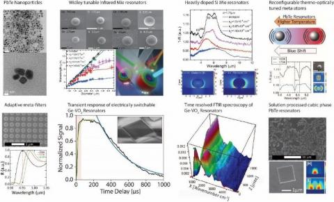
• Light-matter interactions
• Nanophotonics
• Metamaterials
• Plasmonics
• IR nanospectroscopy
• 2D materials -

Prof. Doron Naveh
972-3-531-4657
Graphene Composites for Sensor Applications
- Graphene Electronics
- Two Dimensional Semiconductors
-
Materials Exploration of Optically Active Quantum Spin Defects in Colloidal Nanocrystals
Research in the lab focuses on the synthesis, characterization, and engineering of optically active quantum spin defects in colloidal semiconductor nanocrystals. By combining bottom-up chemical synthesis with advanced optical spectroscopy and spin-based measurements, the lab aims to understand and control spin–photon interactions at the nanoscale. This materials-driven approach seeks to establish scalable, tunable quantum platforms for applications in quantum sensing, communication, and information processing. -

Prof. Avi Pe'er
972-3-531-7482
Broadband Quantum Optics
• Optical bandwidth as a resource for quantum information: Novel schemes for quantum measurement and sources of broadband squeezed light
• Sub shot-noise interferometry and coherent Raman spectroscopy (quantum CARS) using broadband squeezed light.
• Visualization and manipulation of fast vibrational dynamics in molecules with optical frequency combs
• The physics of mode-locked lasers: new sources of ultrashort pulses and frequency combs -

Prof. Amos Sharoni
972-3-738-4516
Phase transitions on the nano-scale
- Spintronics
- New Temperature Coefficient of Resistance (TCR) materials
- Organic/SC hybrid
-
Prof. Issai Shlimak
972-3-531-8176
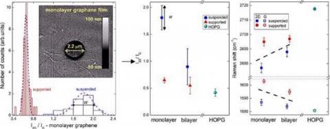
Raman scattering spectra in irradiated graphene
Experimental studies of transport phenomena and electronic properties of disordered solids:
• doped semiconductors
• impure metals
• conducting polymers
• hopping conductivity
• magnetoresistance
• metal-insulator transition
• electron-electron interactions -

Prof. Yoni Toker
972-3-531-7406 -

Prof. Yosef Yeshurun
972-3-531-8369
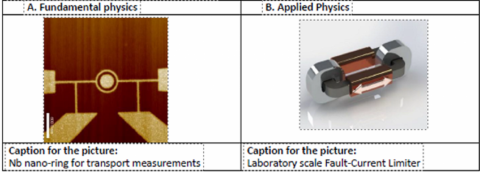
Fundamental physics & Applied Physics
• Condensed matter physics
• Magnetism
• Superconductivity