e-beam Lithography Service
Quantum & photonic nanofabrication
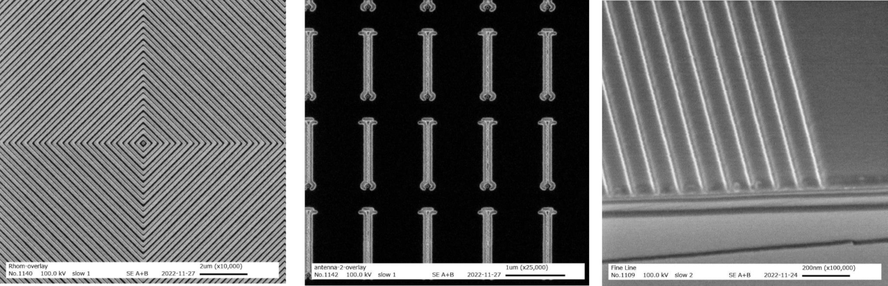
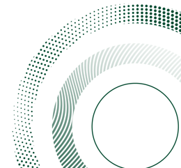
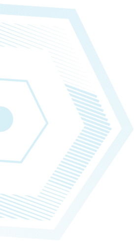
High-resolution e-beam lithography system with 100 keV acceleration voltage for sub-10 nm patterning on electron-sensitive resist-coated substrates.
BINA's Fabrication Unit welcomes both industry professionals and researchers – providing state-of-the-art equipment, expert support, and customized solutions. We’re here for you!
Contacts: Mrs.Irina Pozin, irina.pozin@biu.ac.il
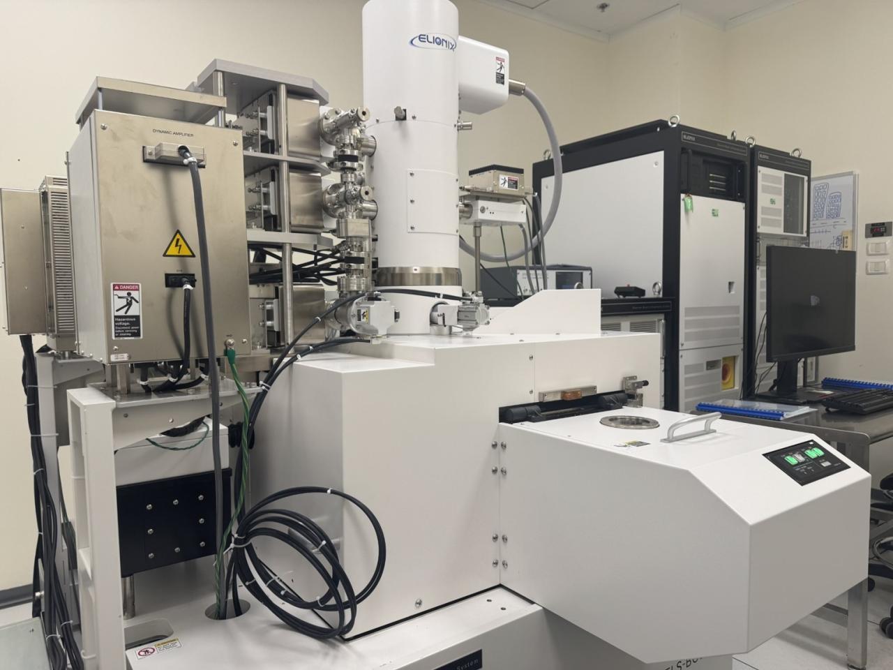
Model: Elionix ELS Boden 100
Manufacture: Elionix
Description: e-Beam lithograpy with 100KeV Acceleration voltage for sub-10 nm resolution
EBL is a direct writing technique that uses an accelerated beam of electrons to pattern features down to sub-10 nm on substrates that have been coated with an electron beam sensitive resist. EBL span a wide range of nanostructured devices including electronic devices, opto-electronic devices, quantum structures, metamaterials, transport mechanism studies of semiconductor/superconductor interfaces, microelectromechanical systems, optical, and photonic devices and more.
Specifications:
- Acceleration voltage 100 kV
- Exposure method Gaussian spot beam, vector scan, and step-and-repeat
- Min. beam diameter 1.8 nm
- Shot pitch 0.2 nm
- Beam current intensity 20 pA ~ 100 nA
- Standard field size 1,000 μm
- Minimum field size 100 μm
- Maximum field size 3,000 μm
- Scan clock 200 MHz
- Max. sample size 8” wafer
- Sample Pre-Alignment station prior to a loading to the vacuum system