

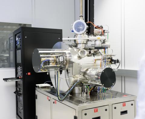
Ion Beam Sputtering System
High quality thin films & multilayers
Versatile ion beam sputtering (IBS) system for high-quality thin film deposition. Ideal for optics, photonics, and microelectronics research needing precise control of thickness, uniformity, and composition.
Contacts: Dr. Olga Girshevitz, olga.girshevitz@biu.ac.il, Mr. Mark Oksman, mark.oksman@biu.ac.il
Model: Intelvac Nano Quest
Manufacture: Intlvac
Description:
Ion Beam Sputtering (IBS) with Ion Assist/Etch is a high-precision thin film deposition technique designed for applications requiring exceptional film quality, such as advanced optical and magnetic coatings. The process operates at low pressure (~10⁻⁴ Torr), allowing sputtered atoms to retain higher kinetic energy due to minimal scattering, which results in:
- Dense, smooth, and pinhole-free films
- Excellent step coverage, even at small thicknesses and on high-aspect-ratio features
- Improved film adhesion and microstructure control through optional ion assist or etching
- This method is ideal for fabricating high-performance multilayer structures where uniformity, surface quality, and reproducibility are critical.
Specifications:
- 4 targets and ION ASSIST/Etch source
- Low pressure sputter deposition (10-4 Torr)
- High quality, smooth, pin hole free films
- Enhanced adhesion and micro-structure control
- Independent control of ion beam parameters allows user to engineer film with desired properties
Materials that may be deposited
- Oxides: SiO2, Al2O3, HfO2, Ta2O5, TiO2
- Metals: Al, Ag, Ta, Ti, Nb
- Others: Ge, Si, Si p-type, Si n-type, Permalloy, ITO, FTO, MOL4, SiC
Last Updated Date : 16/11/2025