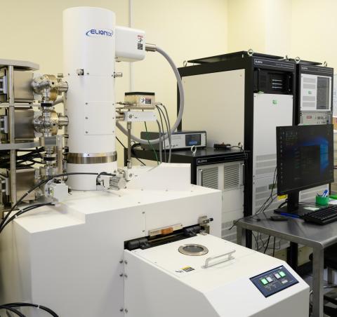
E-Beam Lithography
Contacts: Dr. Musbat Lihi, lihi.musbat@biu.ac.il
Model: Elionix ELS Boden 100
Manufacture: Elionix
Description: E-Beam lithograpy with 100KeV Acceleration voltage for sub-10 nm resolution.
EBL is a direct writing technique that uses an accelerated beam of electrons to pattern features down to sub-10 nm on substrates that have been coated with an electron beam sensitive resist. EBL span a wide range of nanostructured devices including electronic devices, opto-electronic devices, quantum structures, metamaterials, transport mechanism studies of semiconductor/superconductor interfaces, microelectromechanical systems, optical, and photonic devices and more.
תאריך עדכון אחרון : 20/03/2025