Maskless Lithography, MLA
Specifications:
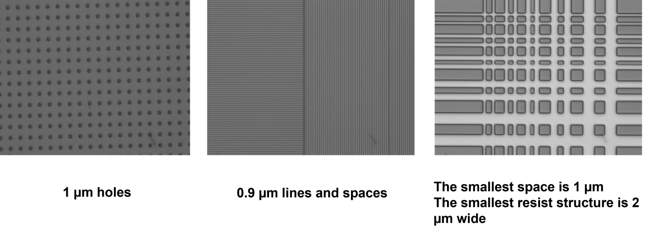
- Minimum structure size 1μm
- Linewidth variation [3σ] 120 nm
- Global 2nd layer alignment [3σ] 500 nm
- Local 2nd layer alignment [3σ] 250 nm
- Light source: Diode lasers 405 nm and 375 nm
- Exposure time 405 nm laser for 4“ wafer 9 min
- Exposure time 375 nm laser for 4“ wafer 20 min
- Max. write speed 375 nm laser 500 mm2 /min
- Max. write speed 405 nm laser 1100 mm2 /min
- Interferometric 200 mm x-y-Stage System with position resolution of 20 nm
- Min. Substrate Size 5 x 5 mm²
- Max. Substrate Size 200 x 200 mm²
- Substrate Thickness 0 to 12 mm
- Temperature controlled flow box Temperature stability ±0.1°


