New in BINA
פרסומים אחרונים

Excellence in Business to Business Electronic Technologies - ZERO EC
Dr. Yossi Abulafia
Bar Ilan Institute of Nanotechnology and Advanced Materials (BINA), Ramat Gan, Israel – created in an unexpected speed a prototype that will revolutionize the approach used in semiconductors. It took only 24 months to come out with the first attempt to combine Zero EC technology within Silicon (a patented technology).
The technology allows electrons to be guided in vacuum, reducing the energy dissipated in the tube to practically zero regardless of the distance (about 10-4 pJ/bit in total). The transfer of data is faster; the usable bandwidth is increased considerably (x1000). In contrary to its homonym, copper that heats and fiber optics that is expensive, this technology feels like an energy boost. The improvements are numerous and permitting a bright future for the semi conducting industry.
https://www.pr-web.com/2021/06/21/development-of-a-revolutionary-electron-prototype/
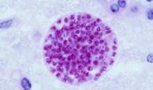

Bar-Ilan University Researcher among International Trio Awarded $4 Million NIH Grant
Prof. Yaron Shav-Tal
Prof. Yaron Shav-Tal and colleagues from the United States will work to shed new light on nuclear dynamics and their impact on the biology of gene regulation.