Atomic Force Microscopy (AFM)
Scanning Probe Microscopy (SPM) is a family of imaging techniques that use a sharp probe that physically scans across a surface while measuring not only topography, but also electrical, mechanical, magnetic properties at resolutions that can reach the atomic level. Atomic Force Microscopy (AFM) offers the capability to image surface topography regardless of sample conductivity.
The Atomic Force Microscopy lab at the BINA Center is equipped with MultiMode NanoscopeV, ICON and Bio FastScan AFM instruments (Bruker, AXS, Santa-Barbara, USA). Two of these instruments (ICON and Bio FastScan) include a stage what enables full navigation and dimensions of the sample up to 8'' in diameter and 12mm in thickness. All systems are equipped with the Integrated Acoustic/Vibration Isolation System, which provides true acoustic isolation for AFM microscopes and allows the Z –resolution 0.2Å.
Using the XY closed loop of the Hybrid XYZ scanner allows accurate and reproducible zooming, as well as high accuracy tip positioning. Using the XYZ closed loop makes it possible to perform highly accurate force-distance curves, current-voltage (IV) curves, and "pulling" techniques, at specific points of high-resolution images. In addition to the measurement capabilities, the scanner is also able to perform nanolithography (both scratching and oxidation) and advanced nanomanipulation applications. It also provides the capability of measuring locally a wide variety of physical properties, some of them with the aid of special modules.
Topography Measurements:
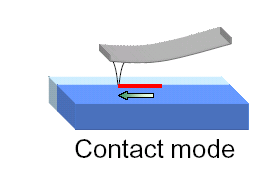
Contact Mode in air and in fluids measures topography by sliding the probe's tip across the sample surface: high spatial resolution can be obtained, but may damage soft surfaces and adsorbed layers.
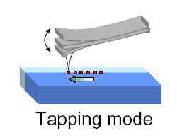
Tapping Mode in air and in fluids measures topography by tapping the surface with an oscillating tip: less destructive to the surface as compared to contact mode. Now this is technique of choice for most AFM work.
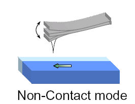
Non-contact AFM measures topography by sensing van der Waals attractive forces between the surface and the probe tip held above the surface: lower resolution than either contact AFM or Tapping Mode.
Special Modules:
The modules are interchangeable in minutes, so it is easy to switch from one application to another.
"Nanoman" Abilities:
- Nanolithography - scratching.
- Nanolithography - oxidation.
- Nanomanipulation of nanoscale objects.
Friction and Elasticity:
- Lateral Force Microscopy measures frictional forces between the probe tip and sample surface.
- Force Modulation measures relative elasticity / stiffness of surface features.
- Phase Microscopy provides image contrast caused by differences in surface adhesion and viscoelasticity.
- HarmoniX Microscopy is the AFM mode that operates simultaneously with TappingMode. A correctly chosen single harmonic can provide compositional mapping of a complex composite material while providing the same resolution as a tapping image (~5nm).
- Nanoindentation is a technique to study the mechanical properties of thin films. It involves forcing a sharp diamond indenter into the surface of a thin film on a substrate, while measuring the force imposed and the corresponding displacement of the indenter. The load and displacement resolution is sufficient to obtain useful mechanical property data as thin film as about 100 nm.
Electrical and Magnetic Properties:
- Magnetic Force Microscopy (MFM): measures magnetic force gradient distribution above the sample surface in the "second pass", with a special magnetic tip.
- Electric Field Microscopy (EFM): measures electric field gradient distribution above the sample surface. EFM is similar to MFM, with a conducting tip and applied tip-sample bias.
- Electrochemical Microscopy (ECAFM and ECSTM) measures the surface structure and properties of conducting materials immersed in electrolyte solution with or without potential control.
- Tunneling-AFM (TUNA): including the local I-V measurements, but with ultra-low current measurement capability, between 80 fA to 120 pA.
- SSRM maps variations in majority carrier concentration in semiconductor materials. A conductive probe is scanned in contact mode across the sample, while a DC bias is applied between the tip and sample. The resulting current between the tip and sample is measured (referencing it to an internal resistor) using a logarithmic current amplifier. This yields a local resistance measurement, which is mapped to generate the SSRM image.
- Torsion Resonance Mode (TR) measures and controls dynamic lateral forces between the AFM probe tip and the sample surface.